
Sony and TSMC Invest 1 Trillion Yen in Kumamoto, Japan… Next-Gen Image Sensor Mass Production Targeted for 2029
Sony Group, the world's No. 1 image sensor maker, and TSMC, the world's largest foundry (contract semiconductor manufacturer), will jointly invest approximately 1 trillion yen (8.9424 trillion won) to produce next-generation image sensors. The two companies aim to develop Kumamoto Prefecture, Japan,
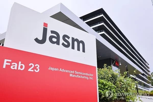
Sony Group, the world's No. 1 image sensor maker, and TSMC, the world's largest foundry (contract semiconductor manufacturer), will jointly invest approximately 1 trillion yen (8.9424 trillion won) to produce next-generation image sensors. The two companies aim to develop Kumamoto Prefecture, Japan, into a key hub for next-generation sensor production.
Joint Venture to Be Established Within Fiscal 2026… Sony 60%, TSMC 40% Stake The two companies will establish a joint venture within fiscal 2026 with Sony holding a 60% stake and TSMC 40%. The production base will be the Sony Semiconductor Manufacturing plant located in Koshi City, Kumamoto Prefecture, where large-scale development facilities and production lines will be built. Subsidy discussions with the Japanese government are also underway. The joint venture aims to begin mass production of next-generation image sensors by 2029.
Kumamoto Prefecture offers favorable conditions for semiconductor manufacturing, with abundant water resources and renewable energy-based power. Multiple production facilities, including TSMC subsidiary JASM, are already in operation, and Sony and TSMC plan to continue expanding their investments in the region.
First Joint Production System… 'First Step in Fab-Light Strategy' This collaboration marks the first transition from the existing division-of-labor structure to a joint production system. While Sony has traditionally developed and produced image sensors in-house, outsourcing only some computational processing semiconductors to TSMC, the two companies will now produce jointly through the new venture. However, Sony's core image sensor manufacturing technology is not expected to be disclosed to TSMC.
With manufacturing equipment and factory construction costs rising amid the spread of AI, Sony's strategy is to share the investment burden with TSMC to improve efficiency. Sony President and CEO Hiroki Totoki evaluated this collaboration as the first step in its 'fab-light' strategy.
Targeting iPhone to Physical AI Markets… Preparing for Intensifying Competition The new sensors will initially be supplied for high-performance cameras in Apple iPhones, and in the long term, will target the 'physical AI' market controlled by AI, such as robots and autonomous vehicles. Image sensors are semiconductors that convert light entering through a camera lens into electrical signals, and are essential for visual recognition in smartphones, automobiles, and robots.
Sony maintains over 50% of the global market share in the CMOS image sensor market. However, with Samsung Electronics and China's OmniVision fiercely pursuing through massive investments, Sony aims to widen the technological gap through its collaboration with TSMC. Competition has indeed intensified, as Samsung's foundry business secured orders for Apple iPhone image sensor semiconductors last year.
TSMC Pursues Taiwan Concentration and Japan Diversification Strategies Simultaneously TSMC is diversifying geopolitical risks by expanding its production bases in Japan. Its strategy involves concentrating on the production of advanced 2-to-3-nanometer (nm) semiconductors in Taiwan, while expanding production facilities in Japan utilizing government subsidies and local resources. TSMC's annual capital investment reaches 10 trillion yen (approximately 89.424 trillion won).
Meanwhile, TSMC recently completed and began operating a next-generation semiconductor packaging technology (CoPoS) production line at its Chiayi Advanced Packaging Plant 7 in Taiwan. It is expected to take about a year for the technology and yield to stabilize. The company is also considering remodeling two AUO factories in the Central Taiwan Science Park into advanced packaging facilities.
The construction of a 1.4nm process semiconductor plant in Taoyuan, Taiwan, which was scrapped in 2023 due to local opposition, is also being pursued again on a 104.19-hectare scale. Three plants in total are planned for the site: two 1.4nm factories and one FOPLP process factory.
Driven by the recent boom in the semiconductor industry, TSMC's consolidated revenue in July reached approximately 467.58 billion New Taiwan dollars (about 21 trillion won), a 44.7% increase compared to the same period last year.
CBC Globe publishes verified stories with editorial review, source checks, and tenant-specific publication standards.
Related Articles
KFA Closes Applications for Interim Coach Hiring... Evaluation Committee to Be Formed This Week, Appointment in August

U.S. Commerce Secretary Howard Lutnick Cites Korea Zinc's U.S. Critical Minerals Investment (Project Crucible) as Key Example
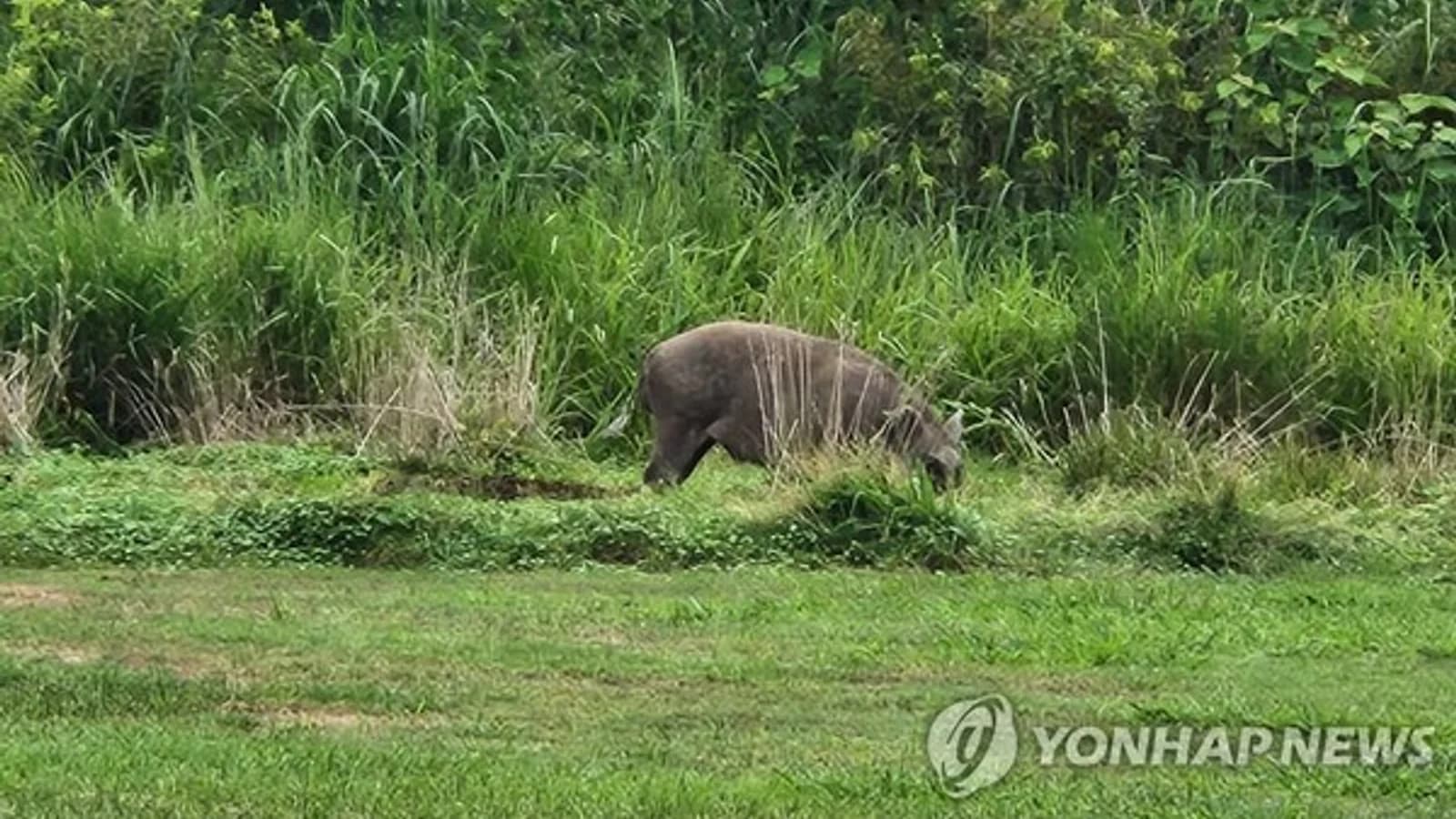
100kg Wild Boar Appears at Golf Course in Seogwipo's Pyoseon-myeon... Hunter Shoots It Dead, Golfers Evacuate in Commotion
![[On Site] Band YB Heats Up Boryeong Special Stage... 'Sound Planet Festival 2026' Kicks Off in Earnest](/_next/image?url=https%3A%2F%2Fmedia.cbcglobe.com%2Ftenants%2Fcbc00000-0000-4000-8000-000000000001%2Fmedia%2Fcbc%2F2026%2F08%2F596844%2F28e68c387d9f6d0b%2Fvariants%2Fhero.webp&w=1920&q=75)